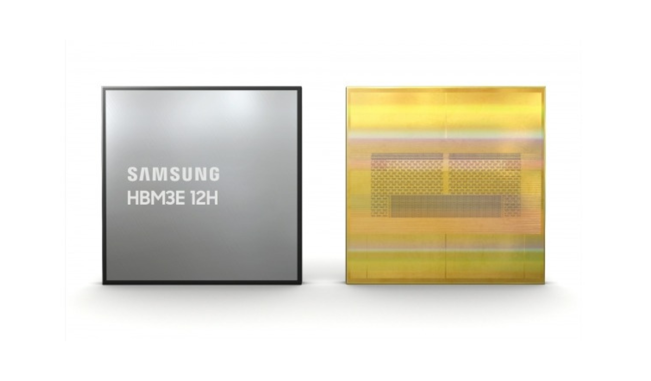
Samsung has dualized its next-generation HBM development organization to strengthen its high-bandwidth memory (HBM) competitiveness. HBM4, which is scheduled for mass production next year, will be exclusively managed by the HBM development team. HBM3E is handled by the DRAM design team that was responsible for developing existing HBM. Through this strategy, Samsung Electronics plans to develop next-generation HBM faster than its competitors.
Samsung dualized its next-generation HBM development
Samsung is focusing on the development of HBM4, the 6th generation HBM, through the HBM development team newly established in March. Samsung Electronics announced in its 2023 fourth quarter conference call held in January that it plans to begin sampling of HBM4 next year and mass production in 2026. However, as SK Hynix, a major competitor, announced a roadmap to begin mass production of HBM4 12-layer products starting in the second half of next year, there are also observations that Samsung Electronics’ HBM4 mass production period may be earlier than planned.
An official familiar with Samsung Electronics said, “The recently newly established HBM development team is focusing on HBM4,” and added, “For HBM3E, the DRAM design team that was previously in charge of HBM development is working hard to develop and mass produce it.” He said.
The HBM Development Team is a new organization established by Samsung Electronics in March to improve HBM competitiveness. Lee Jeong-bae will be placed under the direct control of Samsung Electronics Memory Business Division President (President). The position of head of the development team is held concurrently by Hwang Sang-jun, head of the DRAM development department (vice president). Recently, an in-house job posting (job transition system) was implemented to recruit manpower.
The reason Samsung Electronics split its HBM4 and HBM3E development organizations is to regain hegemony in the next-generation HBM market. Samsung Electronics disbanded its HBM development team in 2019, and as a result, it lost a significant share of the HBM3 market to SK Hynix.
An official in the semiconductor device industry said, “Samsung Electronics predicts that it will be able to reverse HBM market share starting with HBM4,” and added, “Confidence in HBM4 is quite high both inside and outside the team.”
It is believed that there are two main reasons why Samsung Electronics is confident of a turnaround in HBM4. The first reason is the superior bending characteristics of thermocompression (TC)-nonconductive adhesive film (NCF). TC-NCF has the advantage of being resistant to bending compared to competitors as it is performed by applying heat and pressure when stacking HBM. In particular, as the core die thickness must be greatly reduced in products with 16 layers or more, it is analyzed that it may be difficult to control bending for competitors.
The second is the internalization of the advanced foundry. Starting with HBM4, the logic die located at the bottom of HBM must be manufactured using a foundry process. In particular, as the customization needs of major customers such as NVIDIA and AMD are becoming stronger, it is expected that advanced processes of 7 nm or less will be used. In the case of Samsung Electronics, it can be produced through its own foundry. SK Hynix uses the TSMC foundry to produce logic dies.
Kyeong-hyeon Gyeong-hyun, head of Samsung Electronics’ Device Solutions (DS) division (president), also shows confidence in HBM4. President Kyung said on his personal Instagram account last March, “(HBM) has formed a dedicated team, and the team is working hard to improve quality and productivity,” and added, “Through their efforts, HBM’s leadership is coming to us.” I was confident. “Many of our customers want to develop custom HBM4,” he continued, “and they will do that with us.”
